2018 is off to a decent start already, considering that I’ve already accomplished my first personal goal of gathering the “stuff” and setting up to design and build printed circuit boards (PCB’s) in-house. Quite handy for turning designs into actual prototypes and working PCB’s without having to send off the design for someone else to manufacture small quantities of boards.
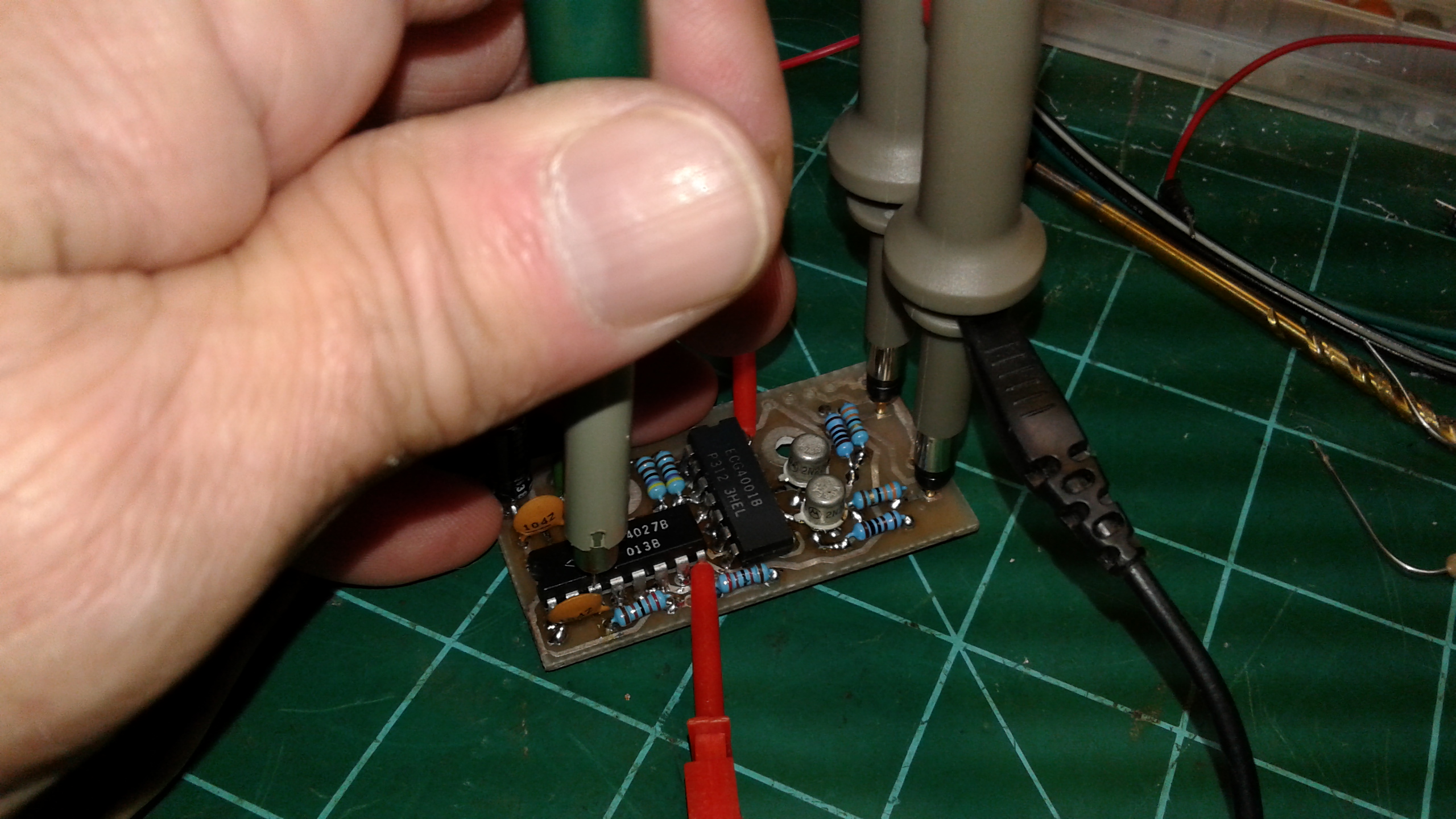
Here’s the first prototype I laid out and created in-house as a test, complete with plated/tinned copper circuit traces. It’s an amplifier keying interface for an Icom IC-706, featuring an optoisolator to isolate the amp’s keying line voltage from the delicate IC circuits in the 706 which are used for external device interfacing. I’d already built a few of these using perf board, but it sure looks neater (and more durable) on a true PCB.
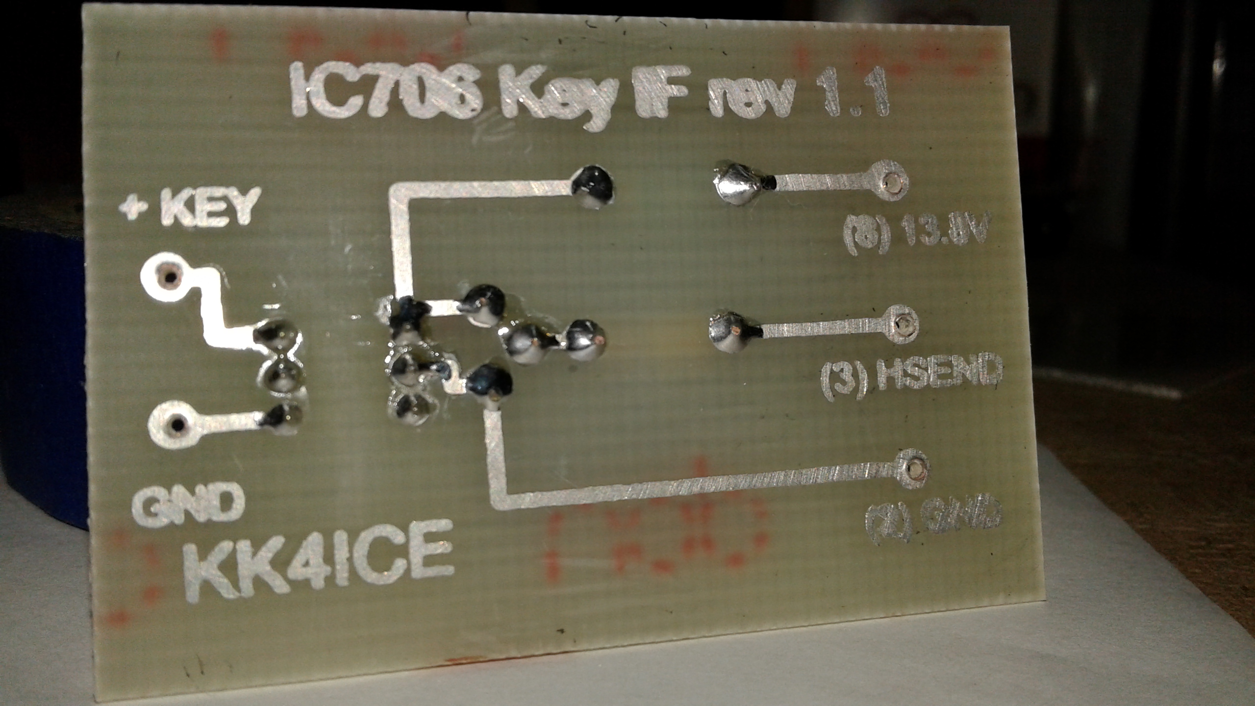
Trace side of PCB. The copper has all been tinned/plated to protect if from corrosion and to make soldering easier and more secure.
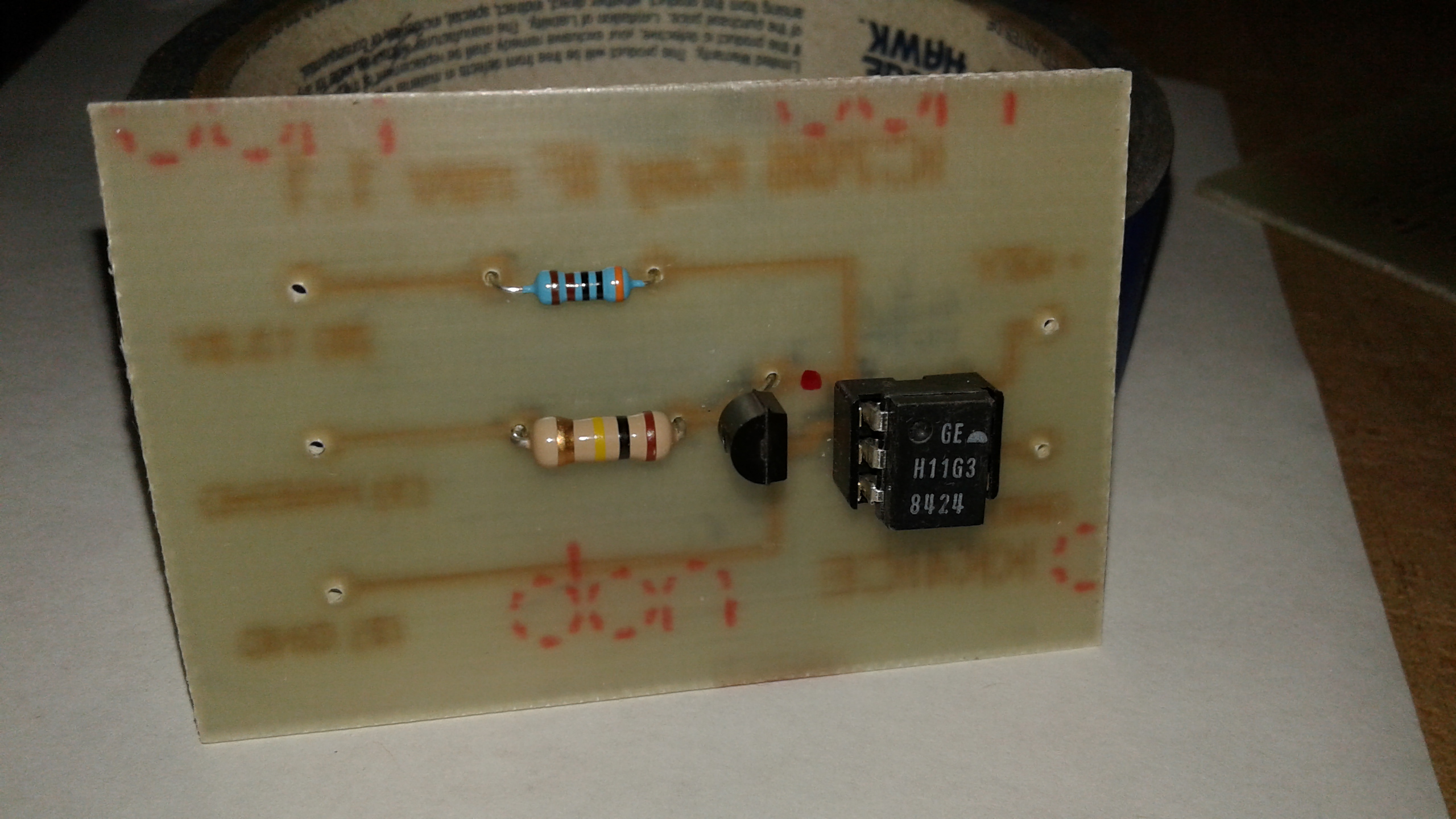
Component side of PCB.
Recent Comments