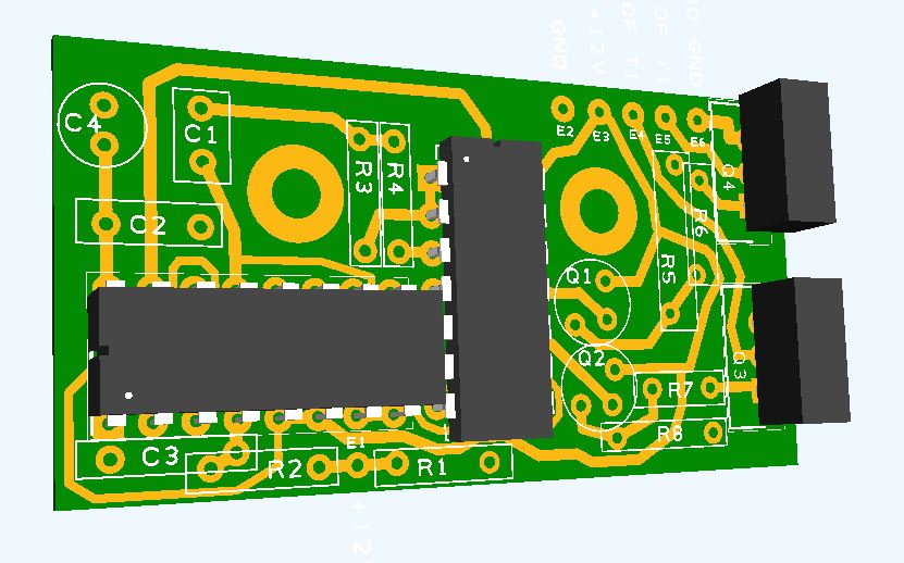
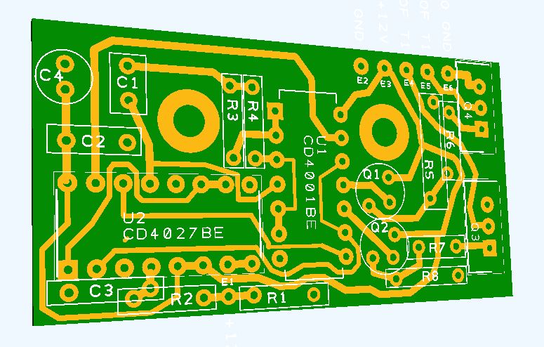
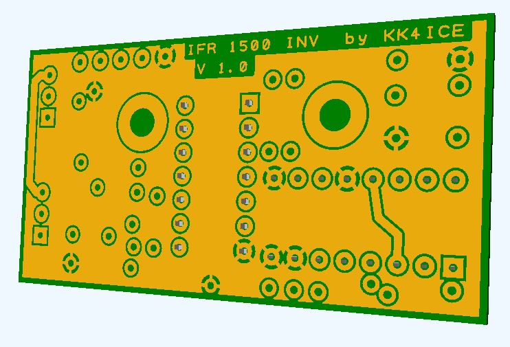
3D view of top of board design.
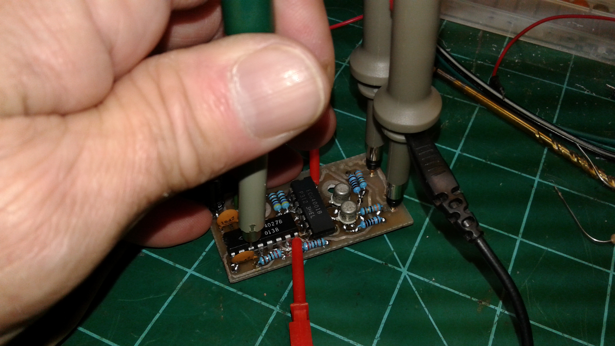
IFR FM/AM-1500 Inverter Board recreation. The original board was seriously damaged when one of the IRF521 FET’s went up in smoke. I tried to patch it up and replace the burned out FET, but the board is pretty much a “goner.” The power supply is still getting “bogged down” with this board in place, and I suspect that quite possibly the other IRF521 FET is damaged, along with one or both of the logic IC’s (a J-K Flip-Flop IC and a Dual NOR Gate IC.) Due to the size of the board, the amount of damage, the fact that attempting to replace parts on this board will likely just do further damage (it’s only 1″x2″ in size), and also the fact that doesn’t seem to be one of these boards readily available anywhere, I’ve made the decision to totally recreate the board. It has taken quite some time to recreate the board layout in a PCB CAD program, but after a couple of days of work on it, I have the files ready to attempt fabrication of the board here in the lab.
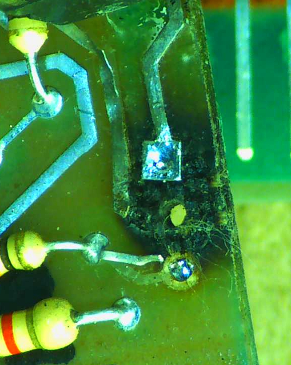
Heat damaged area on top of board due to FET burning out.
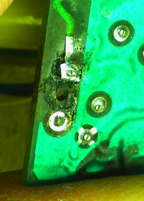
Bottom view of original board with significant heat damage and trace delamination visible.
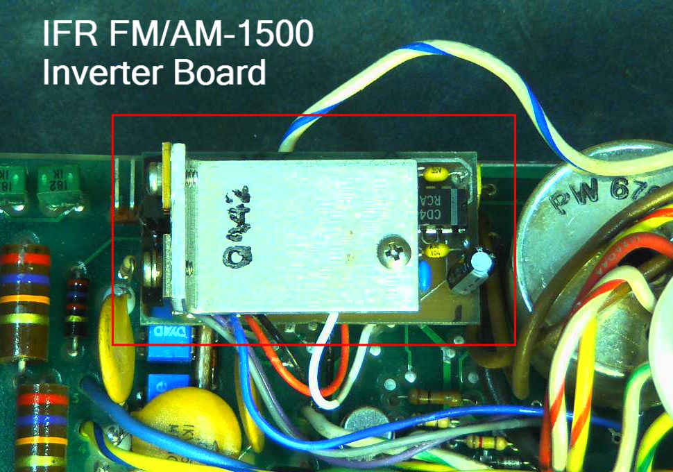
Original inverter board, which “piggyback” mounts on the Oscilloscope Control and Deflection Board
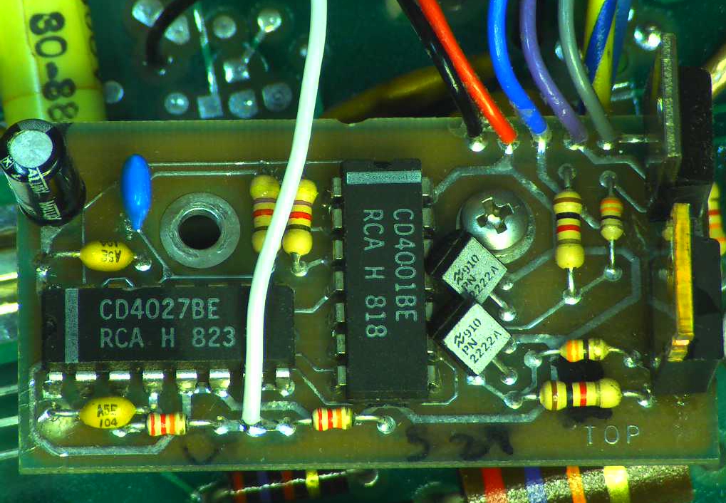
View of original Inverter Board with heat dissipation and mounting plate removed.
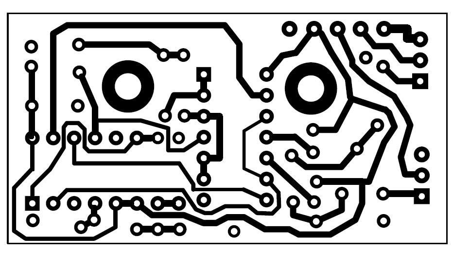
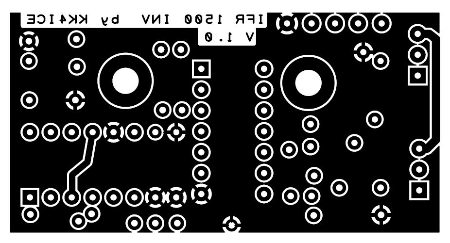
Below are images of the files and graphics which I’ve created in order to fabricate a replacement for the Inverter Board.
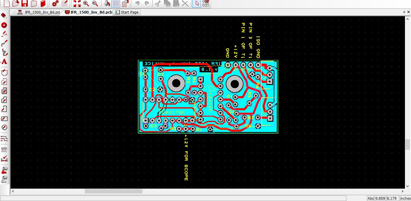
Screenshot of board design in progress.
3D view of top (component) side of board with components hidden, so that only the top copper layer is visible.
3D view of bottom copper layer.
Top copper layer copper graphics file. Note: this graphic will actually have to be reversed before being used for fabricating the board.
Bottom copper graphics.
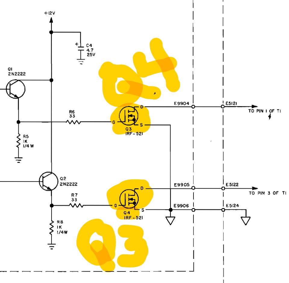
The highlighter marking shows the part identification of the two FET’s as found on the mechanical drawing, which IFR accidentally reversed. I’m sticking with the part number as found on the schematic, flipping the designations of Q3 and Q4 on my design.
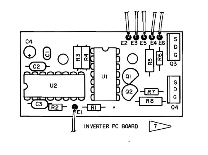
Mechanical drawing as found in the IFR factory Service Manual, which has designations of Q3 and Q4 reversed as compared to their schematic.
In the process of designing the board, I did find a slight error in the service manual documentation from IFR Corporation. The parts labeling and identification on the schematic for the two FET’s (Q3 and Q4) is reversed on the mechanical diagram of the board. No biggie, but I did correct the numbering on my design so that it matches up with the part identification on their schematic.