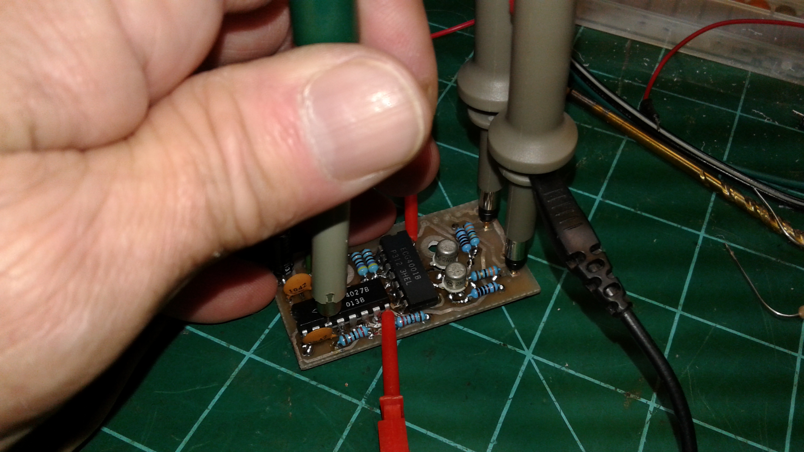

Here’s my recreated board as it stands as of this morning: populated, with the exception of two IRF521 FET transistors, which have not arrived yet.
The project of building in Inverter Board for the IFR FM/AM-1500 Service Monitor from scratch is moving along pretty nicely. At the moment, I’m simply waiting for a supply of IRF521 FET’s to arrive, at which point I’ll just have to add two of them to this board, reinstall the board, and test the machine. Here are some photos of the printed circuit board (PCB) which I built in-house by reverse engineering IFR’s original Inverter Board. After viewing these pics, if you’d like to jump over to my previous post to find out more about the earlier stages of this project and the reason it was undertaken, just follow this link: http://www.kk4ice.com/?p=304. I will post another update after the FET’s arrive and I get them installed, reinstall the board, and test the machine for full functionality again.
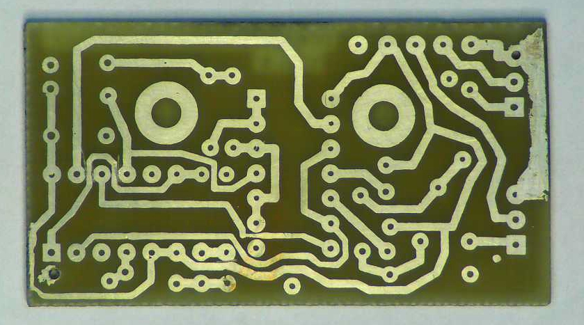
The photos below show the board from the stages of being cut and etched, to the stage it’s at this morning.
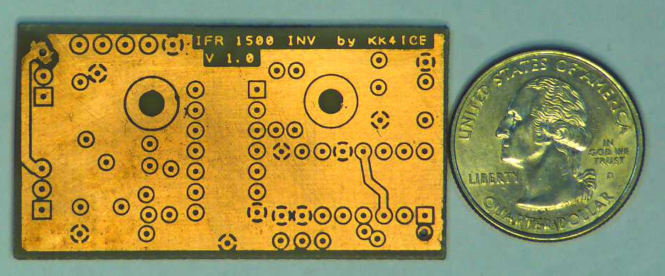
Reverse/ground plane side of board after copper etching was completed. The detail came out quite nicely. For size reference, the labeling text at the upper-righthand corner of the board is only 0.05″ tall, and the font stroke thickness is 0.008″ inches.
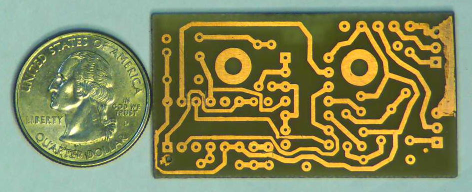
Component side of board after etching, but before tinning.
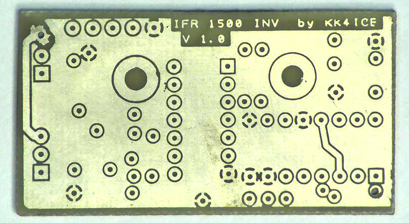
Ground plane side of board after tinning.
Component side after tinning.
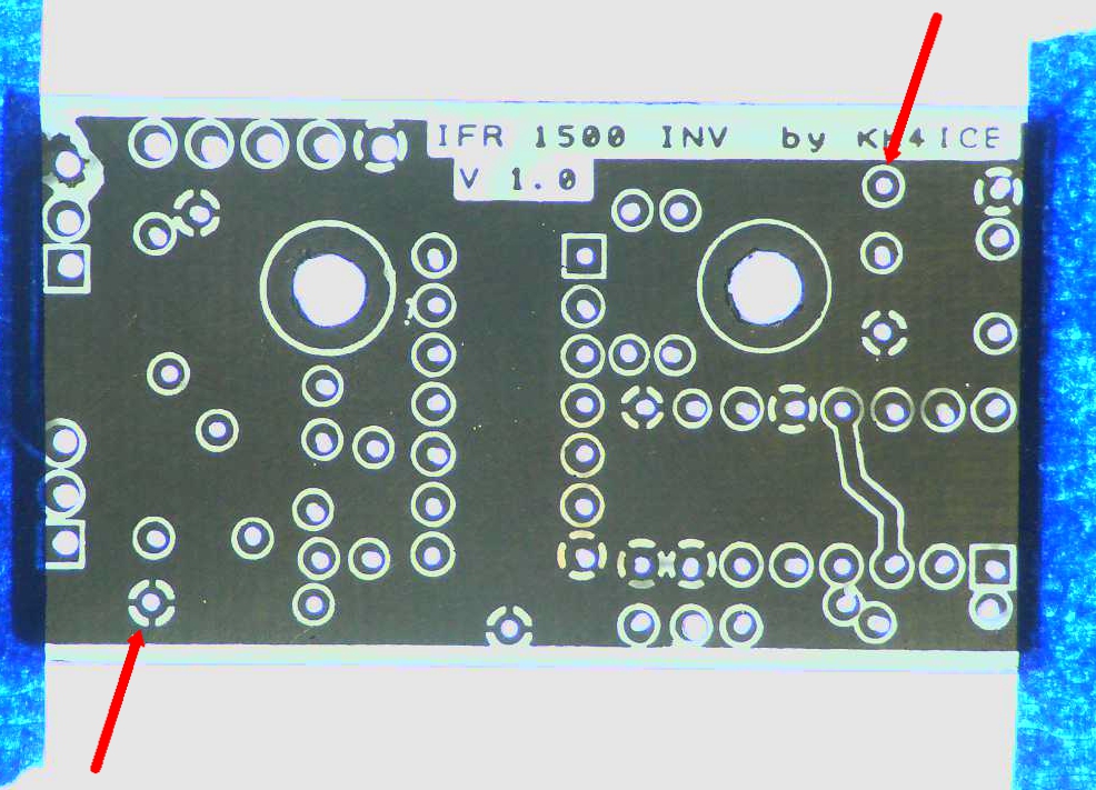
Board viewed on light table for inspection after drilling of thru-holes. The red arrows reference a couple of thru-holes for comparison between the component and ground plane sides, in order to check how well the drilled holes are centered in the pads on both sides.
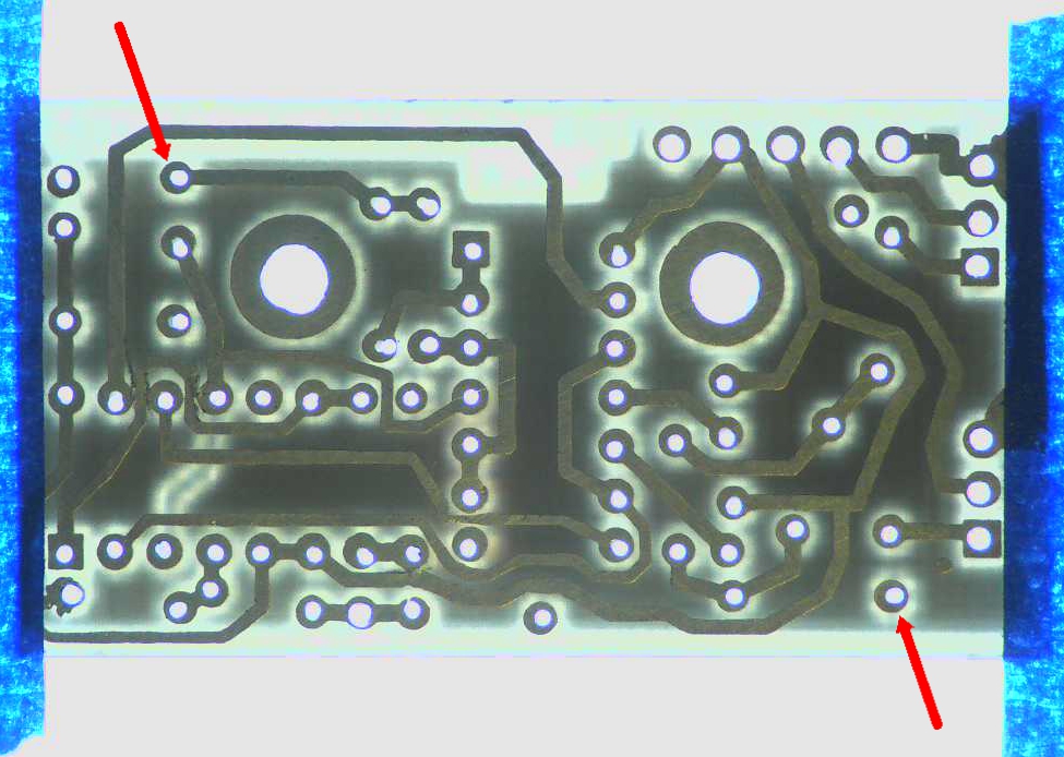
Component side of board being inspected on the light table. As you can see, the pads are well aligned between the two sides of the board.
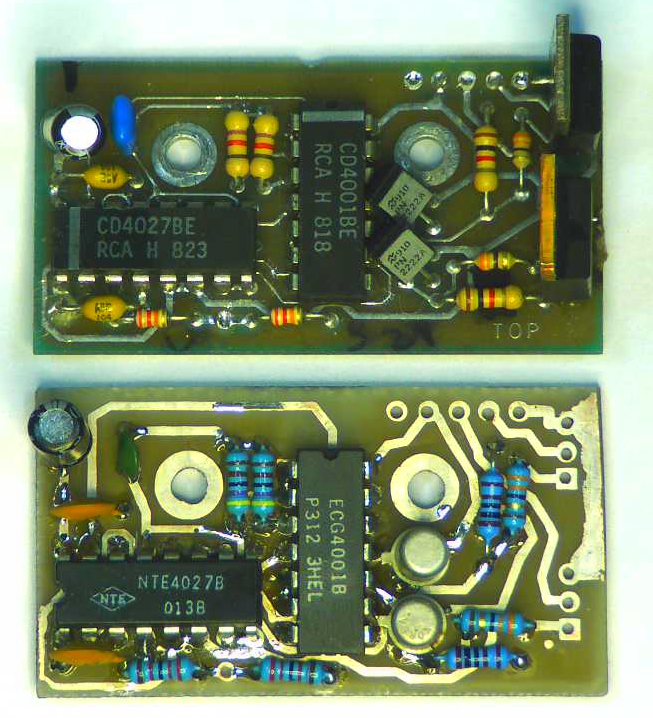
The original, damaged Inverter Board (top) and my reverse-engineered and in-house fabricated board (bottom) after population with all components except the two FET transistors.