I’m still waiting for a batch of the IRF521 FET’s to arrive so that I can install two of them and finish the board up and install it in the IFR FM/AM-1500. Meanwhile, I just conducted the testing of the operation of the board. The purpose of this testing was to confirm that the J-K Flip Flop and NOR Gate section of the board is correctly generating the square waves which will drive the FET’s. This was important because after carefully studying the schematic for the Inverter Board, I did a little further testing on the old, failed Inverter Board to try to figure out WHY the thing actually burned up — more importantly, to answer the question “Did it fail on its own? Or did something else CAUSE it to fail which would require further testing and repair in another area?” The fact that the one of the FET’s on the old board was burned out and I’d already removed both of them from the board was a moot point IF my hunch was right about what had happened. I was solely interested in figuring out the “Why?” part of the equation.
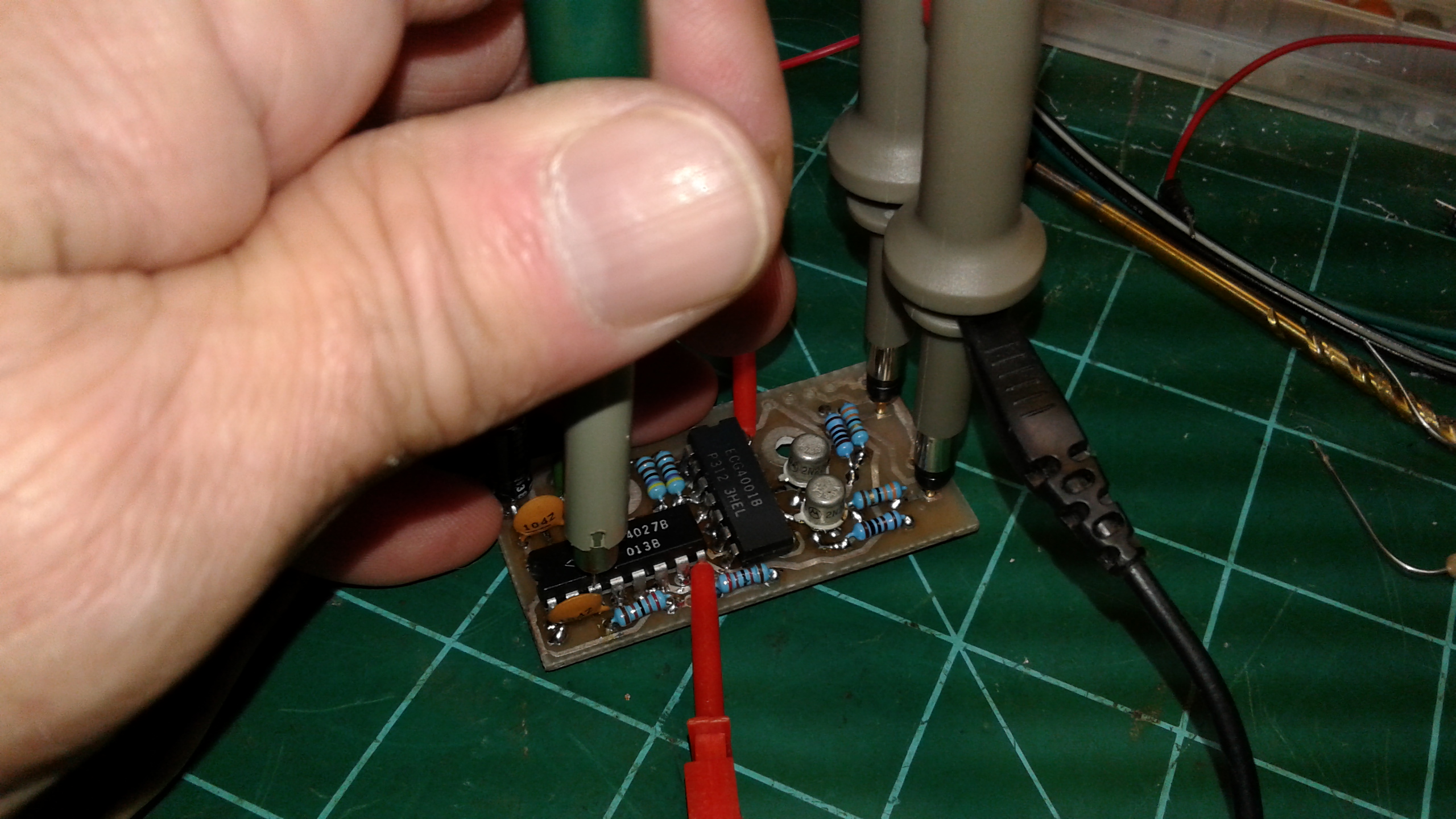
Applying DC power to the logic portion of the board, with three oscilloscope probes attached to view the clock pulse, along with the signals going to the solder pads which will be the Gate (G) connections for the two FET’s on my newly built Inverter Board.
To test the remainder of the old board, I applied to 12V power to the still intact logic section of the board and started looking at the logic signals with an oscilloscope. As it turned out, my hunch was correct. The logic circuit was sending an on/off alternating square wave to drive ONE of the two FET’s; however, the other FET (the one that let all the smoke out and took part of the board and traces with it) was getting a constantly “on” signal to its Gate (G). Since the Drains (D) on the two FET’s are tied together, that told me that the whole idea of this board is to switch the two FET’s on and off in an alternating fashion so that each one is only on while the other one is off, in an alternating or “flip-flop” fashion. If something were to go wrong and either of the two FET’s got turned on constantly it would have at least twice as much current flowing through it as it is supposed to have, potentially exceeding its current/power handling capability. As it turns out, the failure causing the burned out one on this board to be turned on constantly burned it up because it was handling FOUR TIMES THE POWER it was supposed to be seeing (you’ll see why shortly.) I suppose I really should say it wasn’t handling the quadruple power load, because it went out in a blaze of not-so-much “glory.” It stunk up the lab for about two days, in fact.
The way the circuit is supposed to operate is as follows:
- Capacitor C1 (1200) in series with resistors R3 and R4 in a couple of NOR Gate branches in chip CD4001BE forms an oscillating circuit, with a frequency of around 72 KHz. This serves as the “clock” signal for the circuits on the board.
- The cascading of the two J-K Flip Flop circuits in the CD4027BE chip and the way the Reset (R) and Set (S) inputs being tied to +12V and ground respectively produces Q and Q complement outputs of the second J-K Flip Flop which alternate.
- Two additional NOR gates are fed from the Q Complement output of the first J-K Flip Flop and the Q and Q Complement outputs of the second J-K Flip Flop, which results in alternating logic pulses at a frequency of approximately 18 KHz (1/4 of the 72 KHz “clock” pulse frequency.) Each of the pulses has a duty cycle of 25% due to the arrangement of the Flip Flops and the NOR gates.
- The 18 KHz 25% duty cycle pulse output of one of these two NOR Gates is fed to Q1 (a 2N2222 transistor), and the output of the opposite NOR Gate is fed to Q2 (also a 2N2222 transistor.)
- When Q1 sees the approximately 5V logic pulse at its base, collector-to-emitter current flows, causing a voltage to be present across R5. This voltage is fed to the Gate of FET Q3 (an IRF521 N-Channel enhancement mode MOSFET), causing Q3 to be switched “on” at the 18 KHz, 25% duty cycle rate.
- Transistor Q2 drives FET Q4 in the same fashion; however, the “on” period for Q2/Q4 falls exactly in the middle of the “off” period for the Q1/Q3 combination.
- The Source outputs of the Q3 and Q4 FET’s are tied together and fed to the Inverter Board’s E6 connection, which goes to an isolated ground portion of the Oscilloscope Control and Deflection Board. The Drains of Q3 and Q4 are connected to pins 3 and 1 of the CRT yoke connector.
So how does all of this look on an oscilloscope (or a logic analyzer, if you have one) when the board’s logic circuit is operating as it should be?
In the image from the oscilloscope (below) you see the operation of the circuit on the replacement board I build. And it is the correct operation of the circuit. Those pulses you see on the top two traces are the on/off switching signals for the two FET’s. As you can see, each one is only at a logic high state (thus switching its respective FET on) 25% of the time, while the opposite FET is switched off. You can click on the image if you’d like to view it larger.
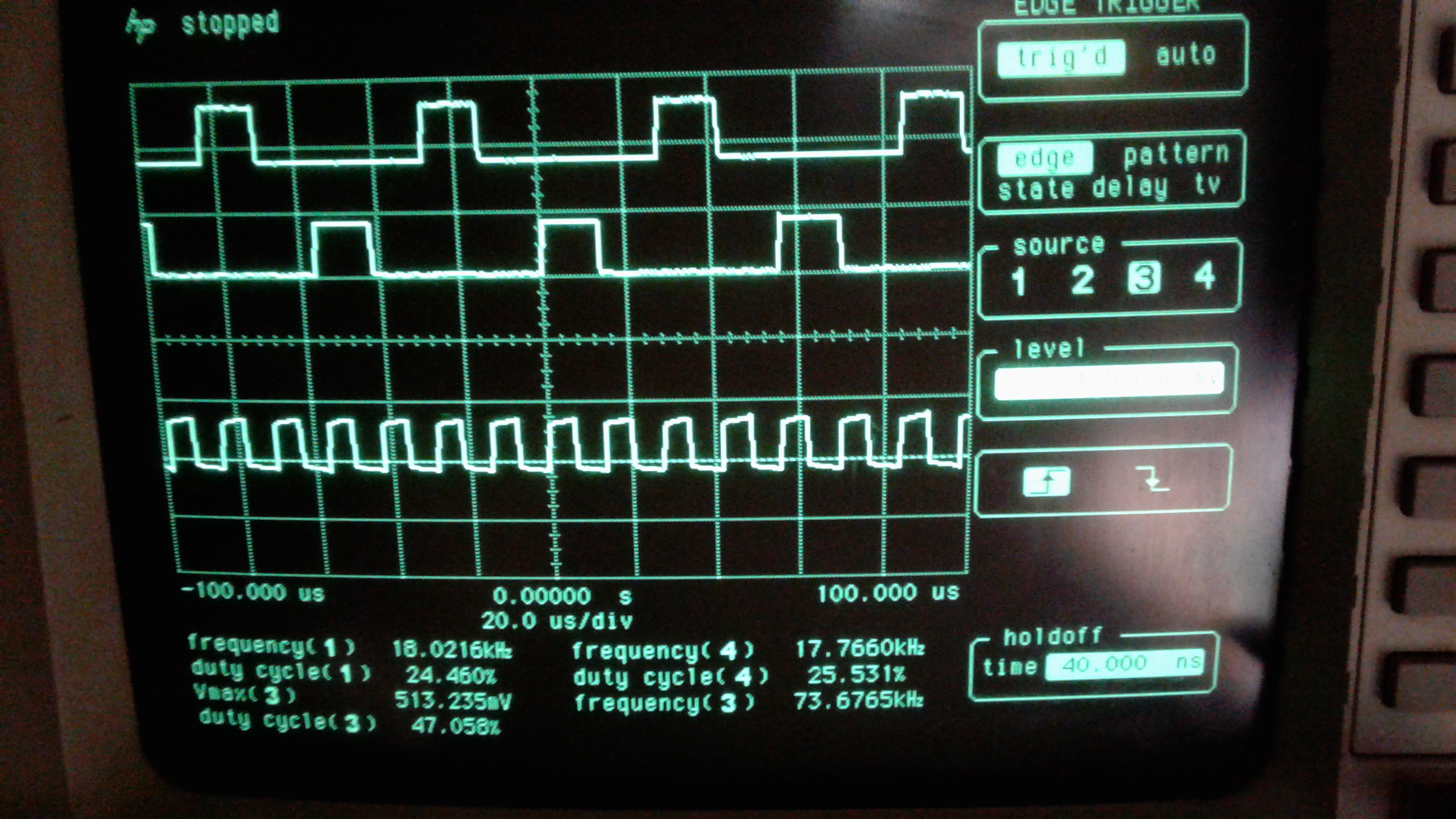
In this screenshot from the oscilloscope, the top trace is the signal to the solder pad for the gate of Q3, the middle trace is the signal for the gate of Q4, and the lower trace is the oscillating clock signal.
So, why was the burned out FET on the old board being switched on constantly instead of only 25% of the time as it was supposed to? Further probing of the logic signals on the the failed board with the oscilloscope revealed that the Q Complement output of the second J-K Flip Flop (pin 14 of the CD4027BE) was flip-flopping between logic high and low as it was supposed to, but the Q output (pin 15) was stuck in a logic high position when it should have been flip-flopping with the Q Complement output. That’s the whole idea behind a J-K Flip Flop. Apparently something failed inside the CD4027BE chip causing the Q output to just “float” to the equivalent of a logic high state. BINGO! I then knew that this failed logic chip was the cause of the fried FET, destroyed Inverted Board, and that awful stench I lived with for a day or two.
Another update to this will be posted after the FET’s get here. Meanwhile, does anyone want to hum the theme from the game show Jeopardy! with me?